Hi. I’ve found a psk interface that I think will work with my tablet and would like to make a PCB for it using the designs supplied by DD7LP on his website. Having only ever made one at school before in tanks of nasty stuff. Is there a way of making a PCB at home for not much money. I’d prefer to do a PCB rather than any temporary looking solution as it will be transported in my rucksack for Sota.
fwiw, I needed a small PCB for a circuit I designed 18 months ago. I had never done anything like this before but was able to do the design on a computer and order three boards online for $20 and had the boards in two weeks (oshpark.com) - these were two layer boards with soldermask and silkscreen and they came out beautifully.
Etching is probably the cleanest solution you’ll be able to achieve at home unless you have a small CNC router available to cut out traces and drill holes for you. Dead bug (a.k.a Manhattan style) circuits, perf board, or proto board can be just as sturdy as a PCB, if perhaps a bit bulkier. With enough solder and epoxy they can actually be even more rugged. Designing your own PCBs can be quite rewarding and is a useful skill to have, though the learning curve with various CAD software can vary. KiCAD is free, open source, reasonably well supported and will provide you with a complete toolchain. Other people will have different preferences and, based on the complexity of your circuit, there may be simpler solutions.
You may find it prudent to get an ‘ugly’ version of your circuit working first to refine the schematic before ordering boards from a fabrication house. There’s also LTSpice, which is a software circuit simulation tool and is quite handy for sorting out bugs before putting solder to iron.
The ham radio 360 podcast guys did some shows on PCB design and ordering them from a PCB making house - it’s probably worth looking up the podcasts at hamradio360.com - they recommend a free PCB design software called Eagle from Autodesk believe.
Thankfully the PCB is already been designed for me and all files are available to download from the URL I posted above. I have been googling etching PCB at home. I think I will make sure it works on breadboard or similar before doing the PCB.
If it were me I’d make one up on Veroboard and that would be it. However it does look rather sexy made from SMD components. It’s years since I etched a board, maybe 18+. IF you really want a board, get the PCB files from the website and send them off and have 5 boards made with masks etc. for £15 or whatever. Make up one for yourself and sell the spare PCBs to reduce your costs.
Ed’s correct that Eagle is the go to shareware/free PCB program. The free version was has limits on the number of tracks and components it supports. It works, there’s loads of tutorials on using it and most prototype PCB companies support Eagle files.
It will be bigger than when it is made with surface mount components. If you haven’t tried before then it may be difficult to make the circuit tiny, but with a only a few components I’d expect to get it easily on a piece 2cm X 4cm.
You could try sketching out a layout on a piece of graph paper.
I presume you know for US$40 you can buy an interface unit ready built and designed to work with the software covered in the presentation from DD7LP (Hmm, I’ve seen a very similar call sign to that somewhere…).
I did check to see if it was you today lol.
Yeah I know but £40 is too steep for my wallet for an interface. I’ve always wanted to make something for ham radio and I think this should be manageable. I can get plenty of help at my radio club if I need to once it’s built. Then I could do a build workshop at the club maybe once I got mine working.
My family history is from Yorkshire and my surname is a Scottish clan name so spending money gives me cold sweats and I don’t understand it.
You might also look into Manhattan style construction. Very flexible and easy to do. (this guy uses commercially made “MePads” which are wonderful, but you can just cut up little squares or rectangles of PC board) https://aa7ee.wordpress.com/tag/qrpme-mepads/ I’m really jealous of his neat layouts! Mine tend to be more “individualistic”
If you are determined to make your own boards, have a look at these vids for the method I use.
I hadn’t heard of Copper Connection before, but after taking a look at the walkthrough video it looks easier to use for simple projects than a lot of other software. I might start using it for home etching, too bad you need to buy a license to get Gerber files out of it. Still, very nice tool.
Since I am only an occasional user of such tools, I need to strike a balance between fully-featured (hard to retain all the skills) and too-simple-to-do-what-I-need. Copper Connection seems to sit in that sweet spot, at least for me. I find that it works well for “noodling”, as Pete Juliano, N6QW calls it when he just moves things around with pencil and paper before starting his actual build. Of all the other tools out there, this is the one doesn’t seem to get in my way while the creative process is going on.
I have found a nice german chap who can provide the PCB for cheap, he does this sort of thing apparently. he even sent me an updated version of the pcb i want.
The way I prototype and still do is to use the toner transfer method using transfer sheets like these from Ebay. It still has some cost associated with it, mainly time. Unless the design is complex or large I don’t bother and go straight to a full design to send out.
With no solder mask, plating etc I can mess around with the design as much as I like. Cut tracks, tomb stone components lift chips up and insert mod wires etc etc.
Once I am happy I’ll re-spin the CAD to either 2 or multi-layer, send it out to a PCB house.
Developing is too expensive and the copper tarnishes unless you plate it, so your project looks terrible in 2 - 3 years time. Much nicer to have a professional mask with top and bottom silk.
Wish I was still at the University of Manchester where I had 2-3 day turn around at no cost at all… they were the days.
Altium Designer 10 is the choice of software I use, not cheap to buy unless your a freelance and recover the costs that is dependent on your profession I guess.
Don’t be fooled into thinking you cannot do SMD. People who moan how impossible it is have no desire to learn the skills needed to do it in the first place, its just patience.
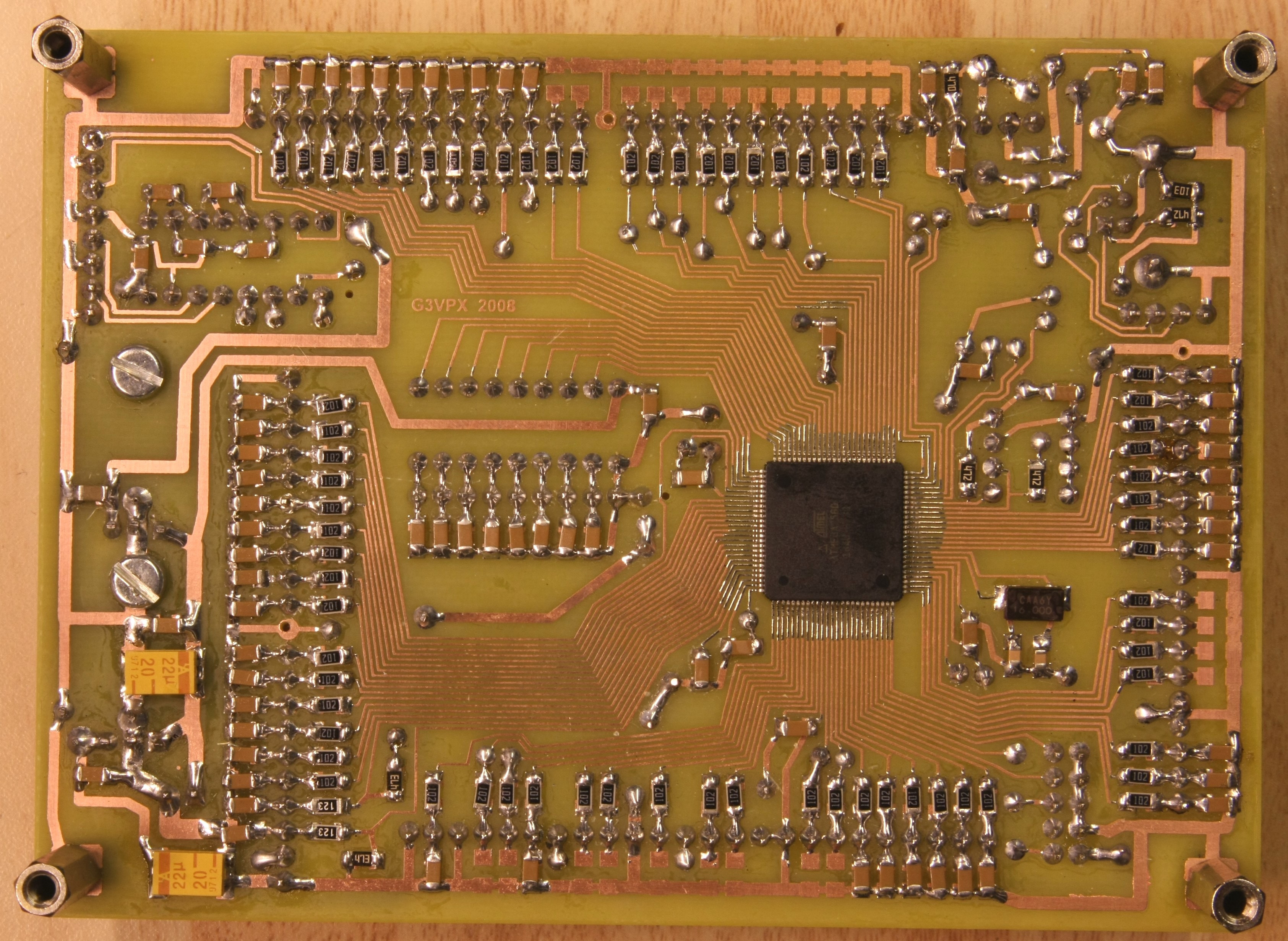
Controller board in Trx_AVR PICASTAR prototyped using home etching techniques on 0.5mm pin pitch. Ian is in his 60’s, age is no barrier either…