AB1PJ - Hello Jim.
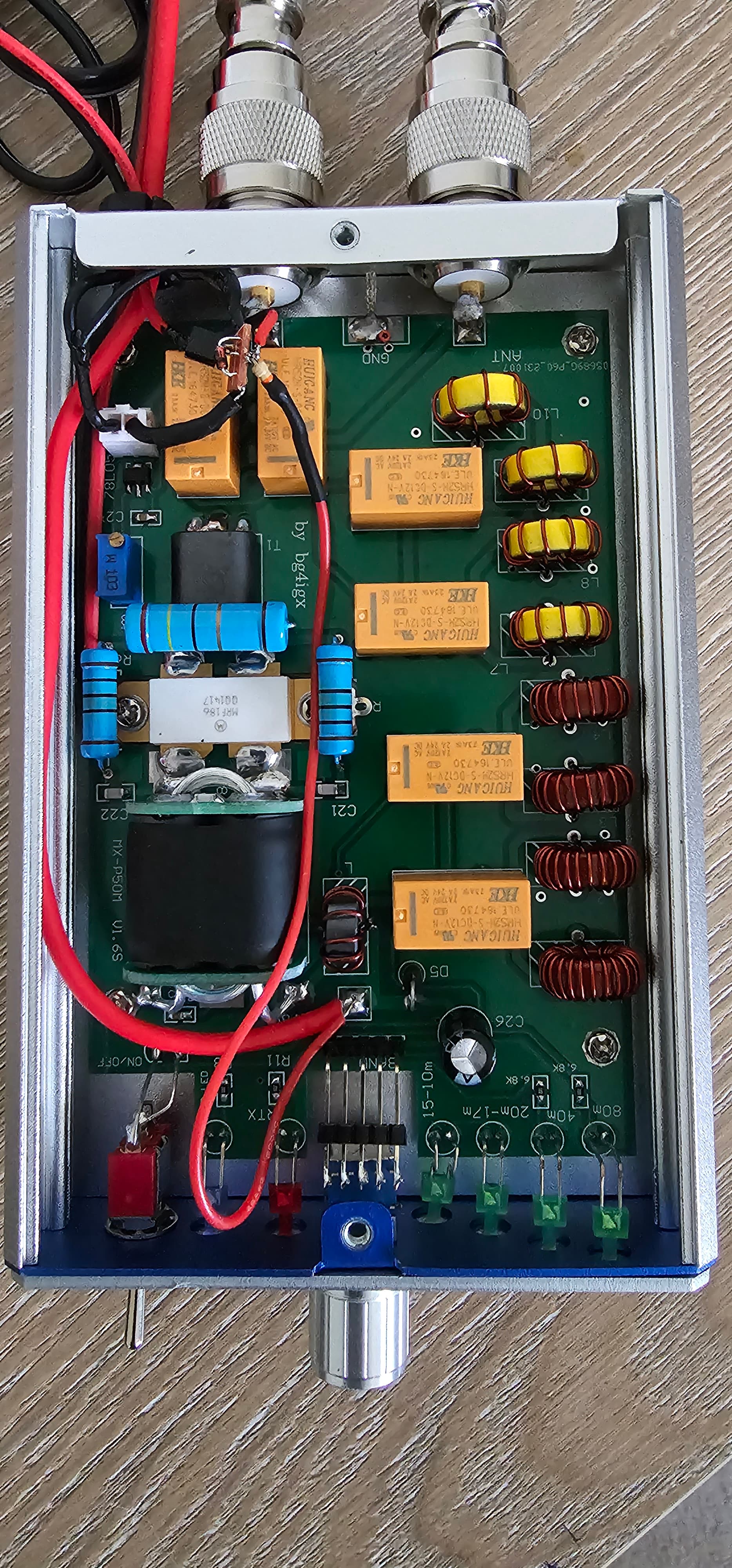
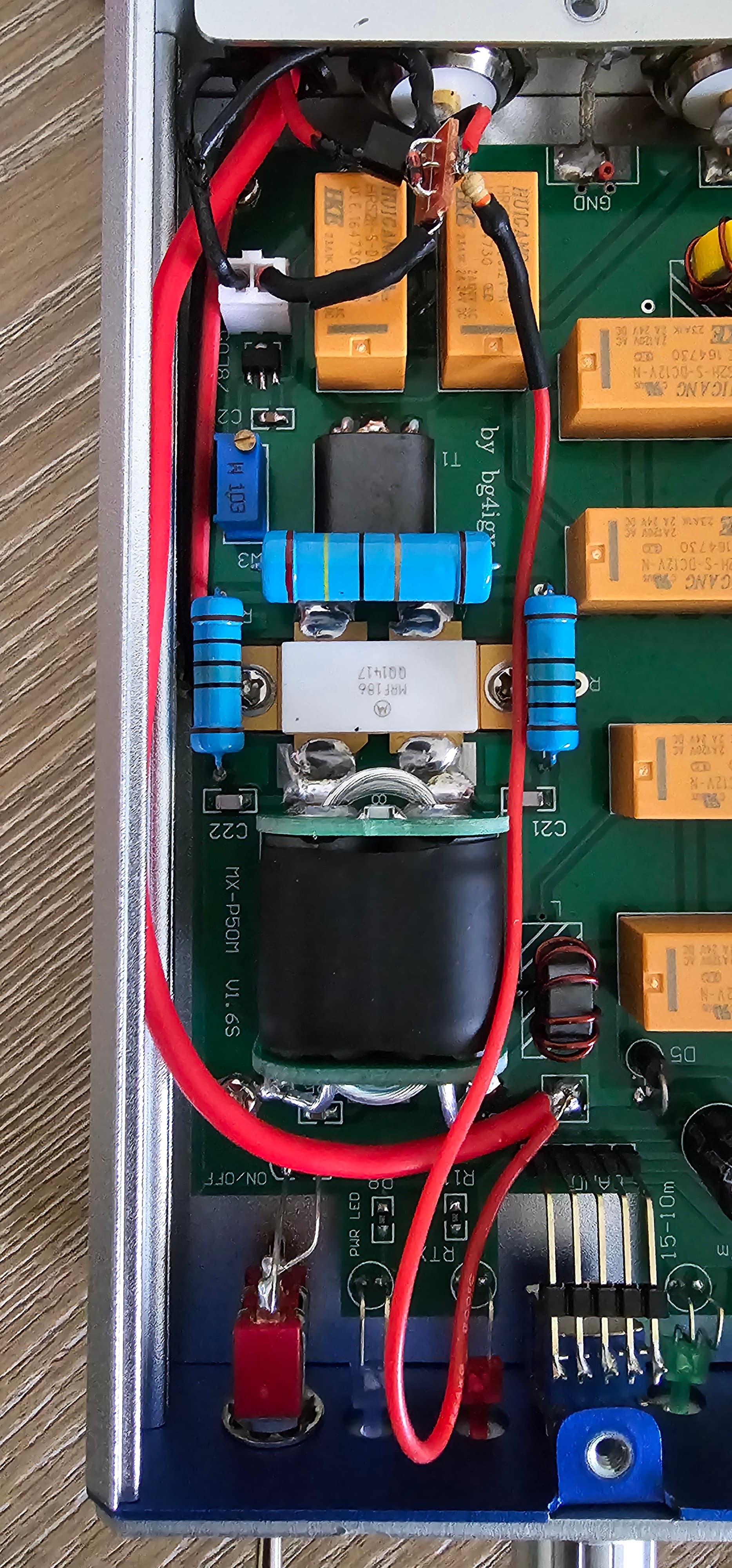
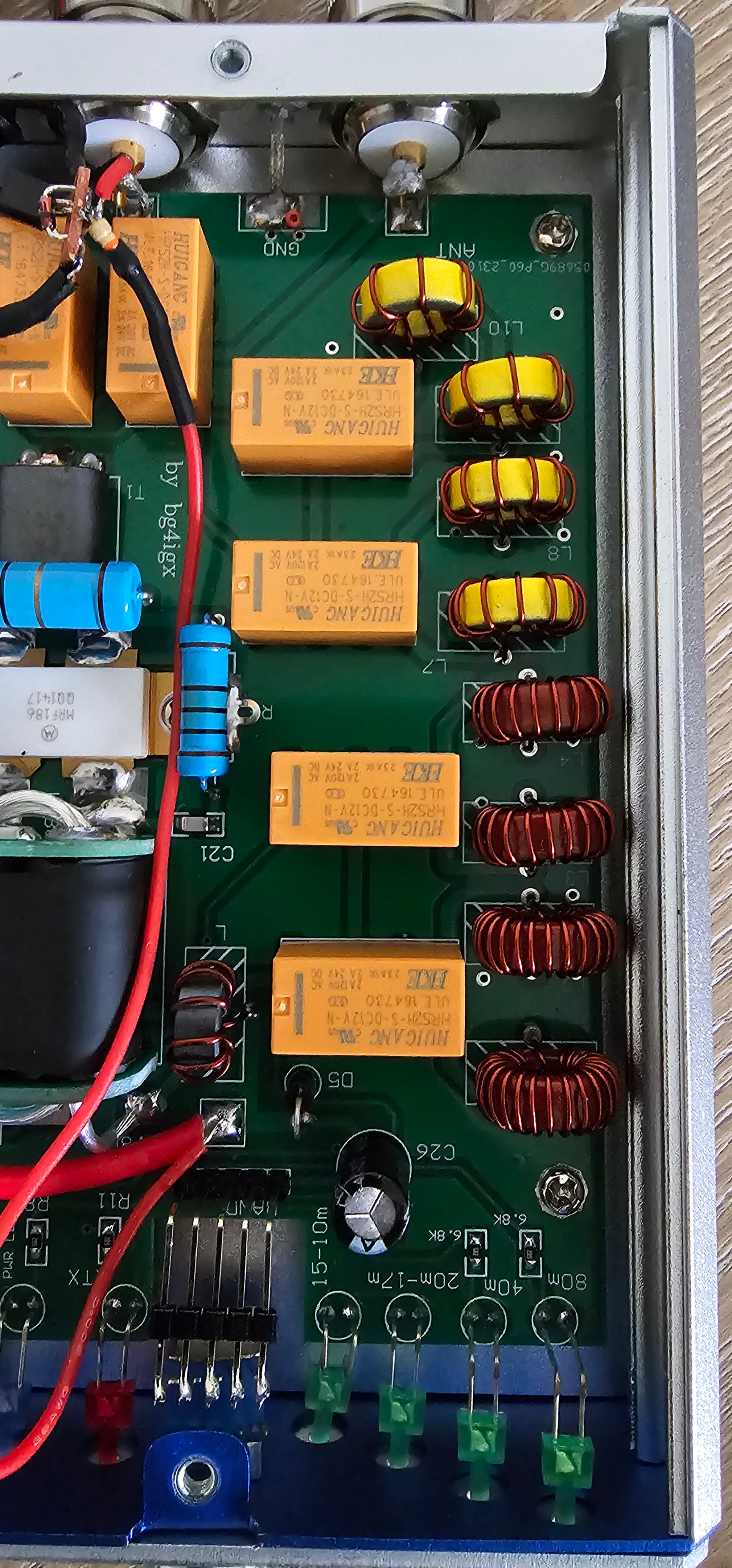
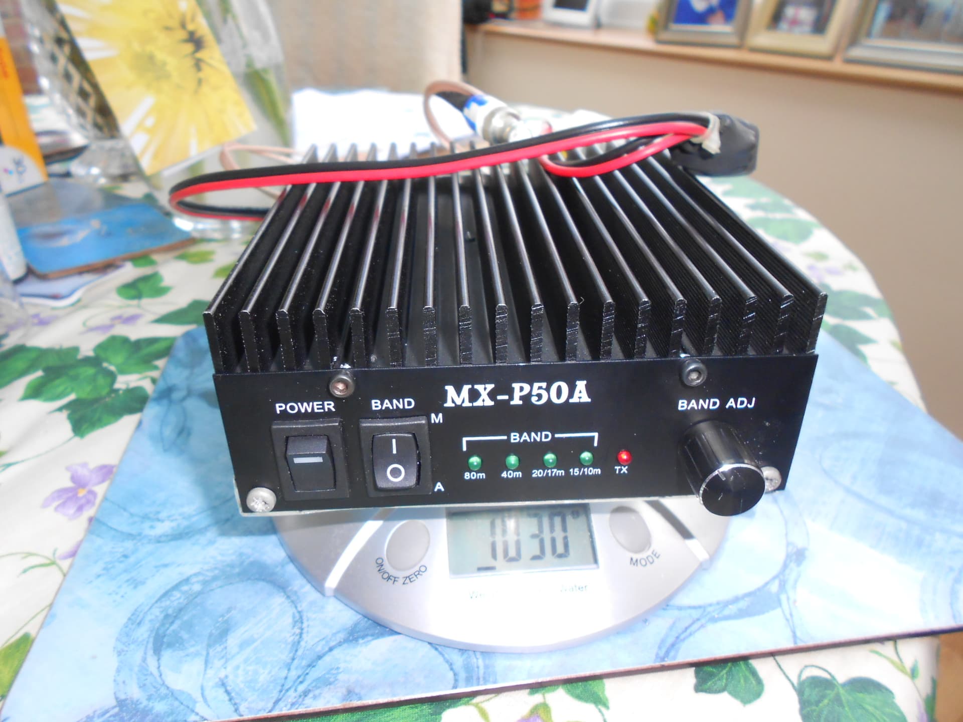
MX-P50M HF 50W Amp / MRF186 RF Power Output Device Replacement
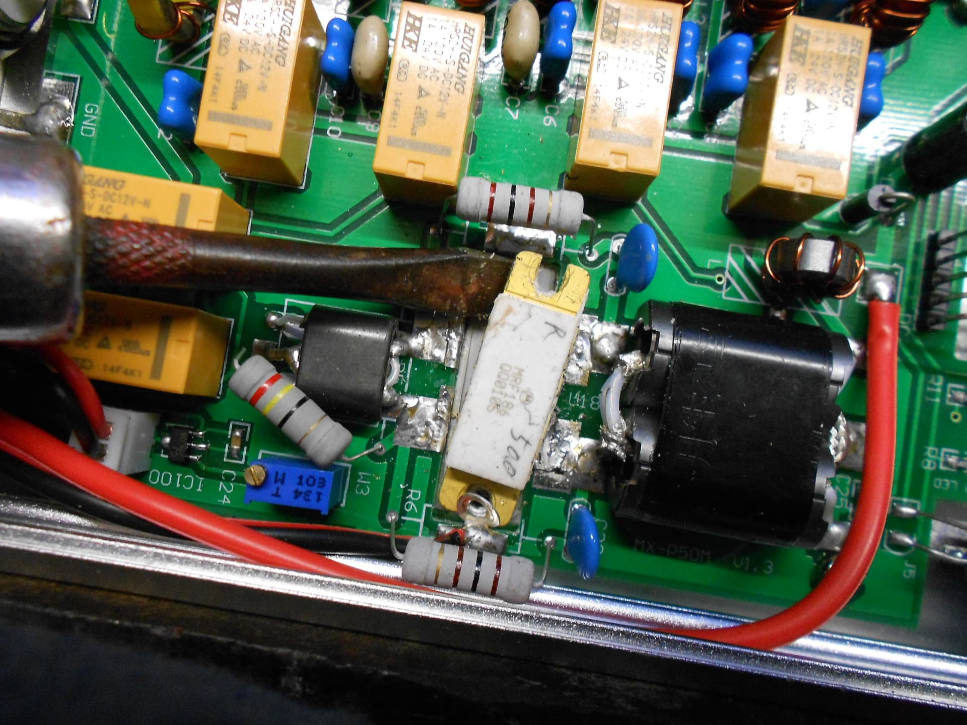
My MX-P50M Amp failed at the end of a CT3 activation. I thought at the time there’d been an antenna mismatch – maybe the wrong links were open in the dipole? Can’t remember.
Anyway my problem was the MRF186 RF power output device. A new one didn’t cost very much – £11 at the time 2017 then I bought two spares at £9 each plus a second MX-P50M amplifier in case it happened again. All from ebay.
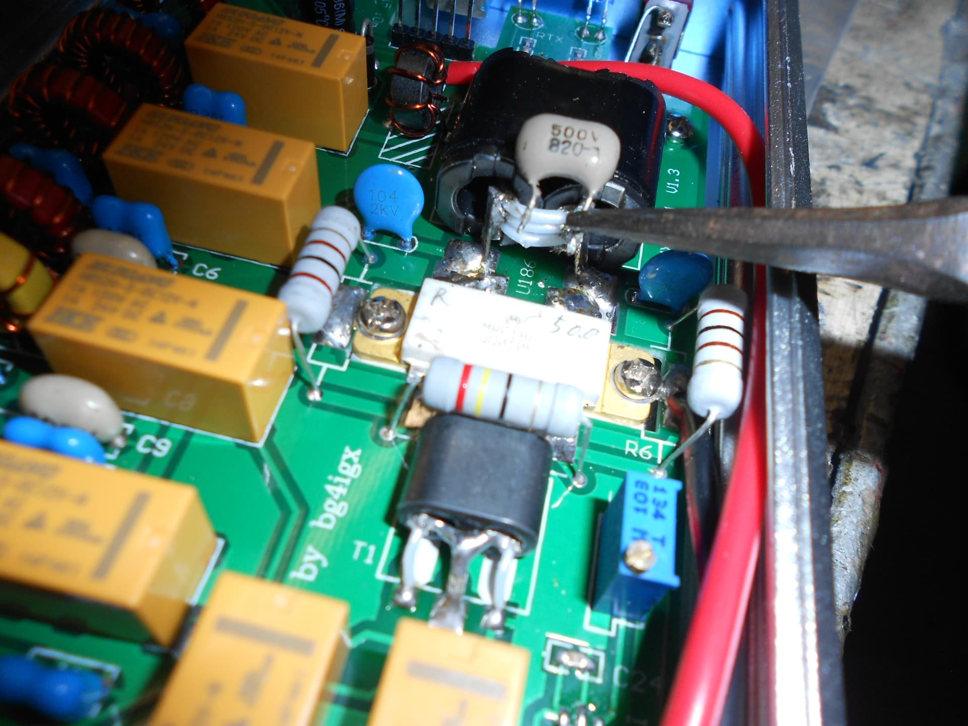
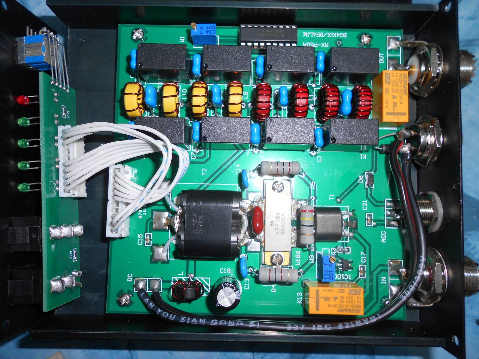
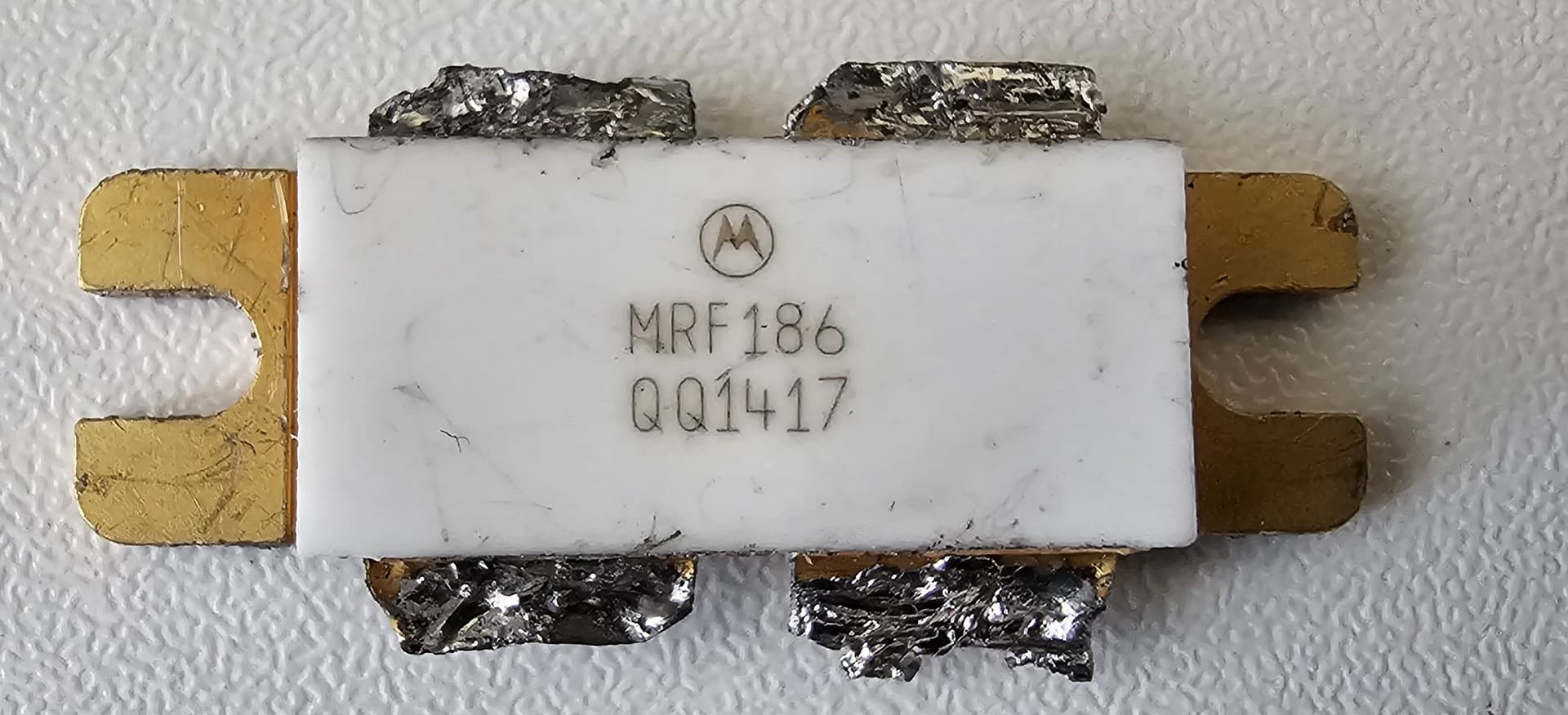
The device consists of a flat copper plate with slots to accommodate screws at each end and a ceramic body. Two copper terminal tags protrude from each side of the ceramic body (five terminal device). They are quite simple to replace. Left to right, with ‘MRF186’ labelling facing you (so you can read it), I’m naming the terminals A & B along the top and C & D along the bottom (closest to you).
In case you need to, this is how I replaced it:
(NB: Take note of which way around it goes before starting)!
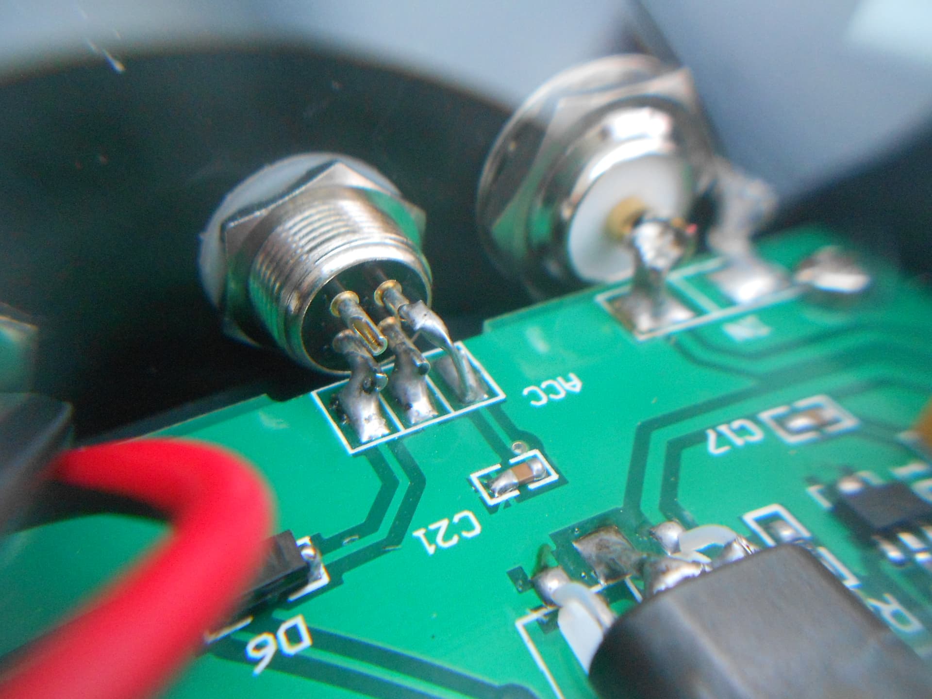
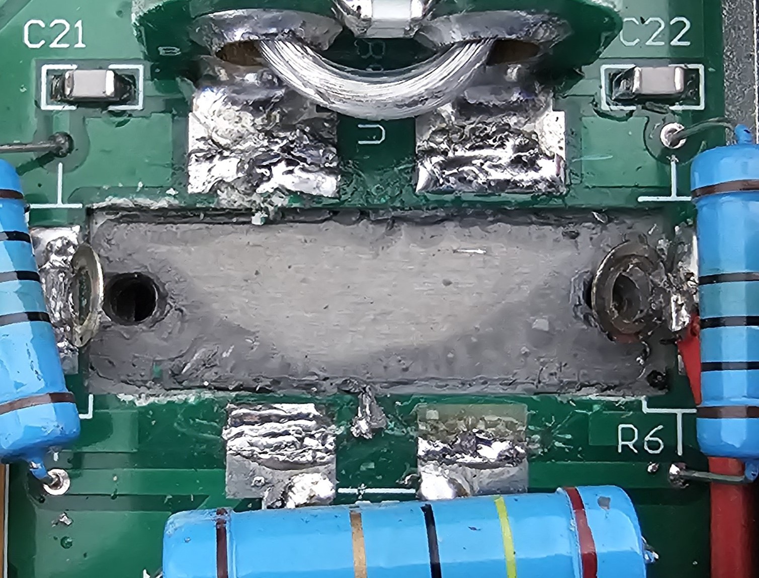
Unsoldered the capacitor across terminal tags A and B and removed for now.
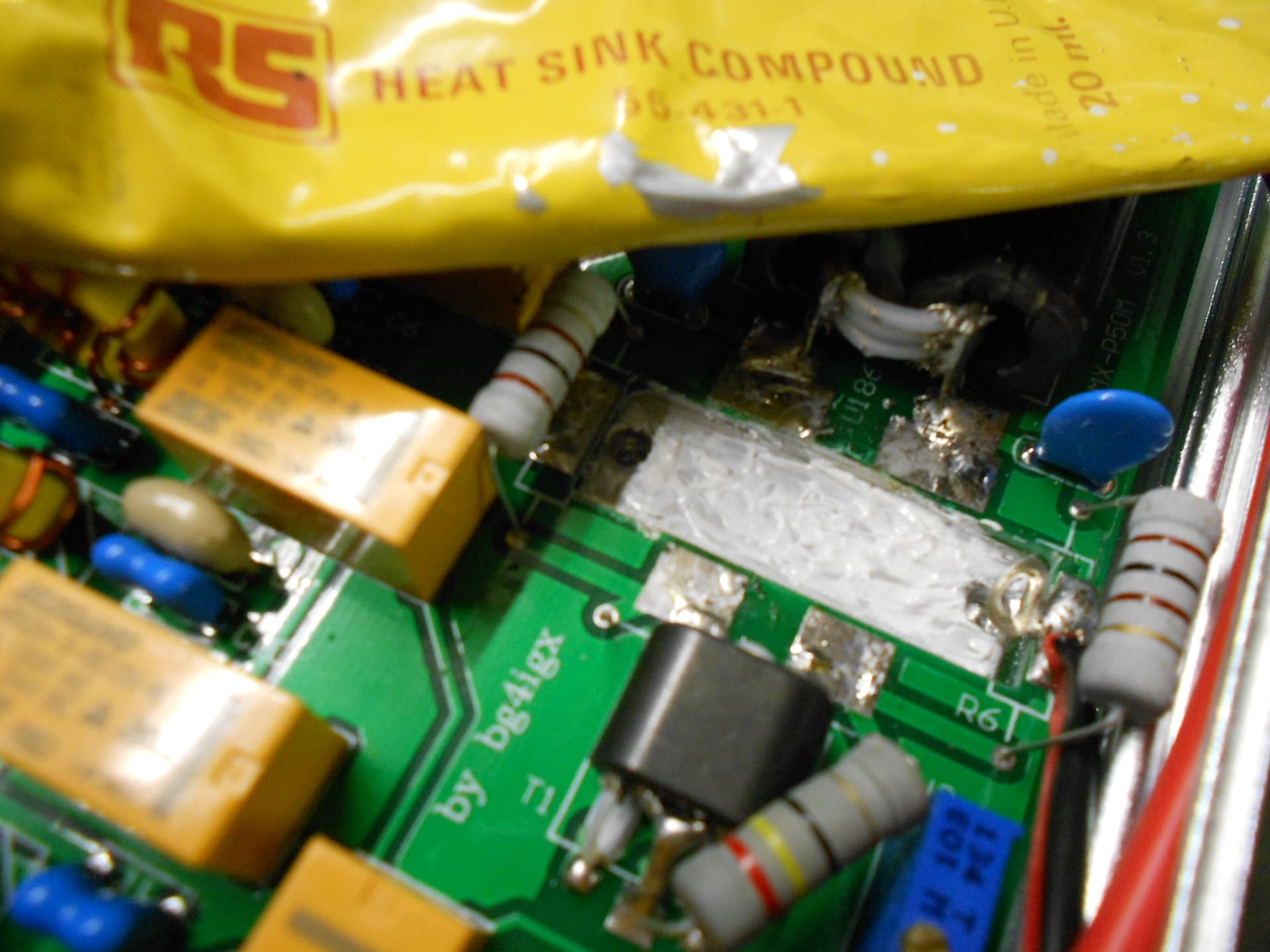
TIP: I found it best to cut through the four terminal tags right up close to the ceramic body of the device using a sharp Stanley knife (new blade – 4 cuts). This was after messing around for too long with a 50W soldering iron and a solder sucker.
Removed the two securing screws.
Gently levered up the blown device using a flat bladed screwdriver. To avoid damage to the PCB, if it doesn’t lift readily, find out why!
Removed what was left of the old terminal tags from the PCB pads using the soldering iron and a sucker.
……
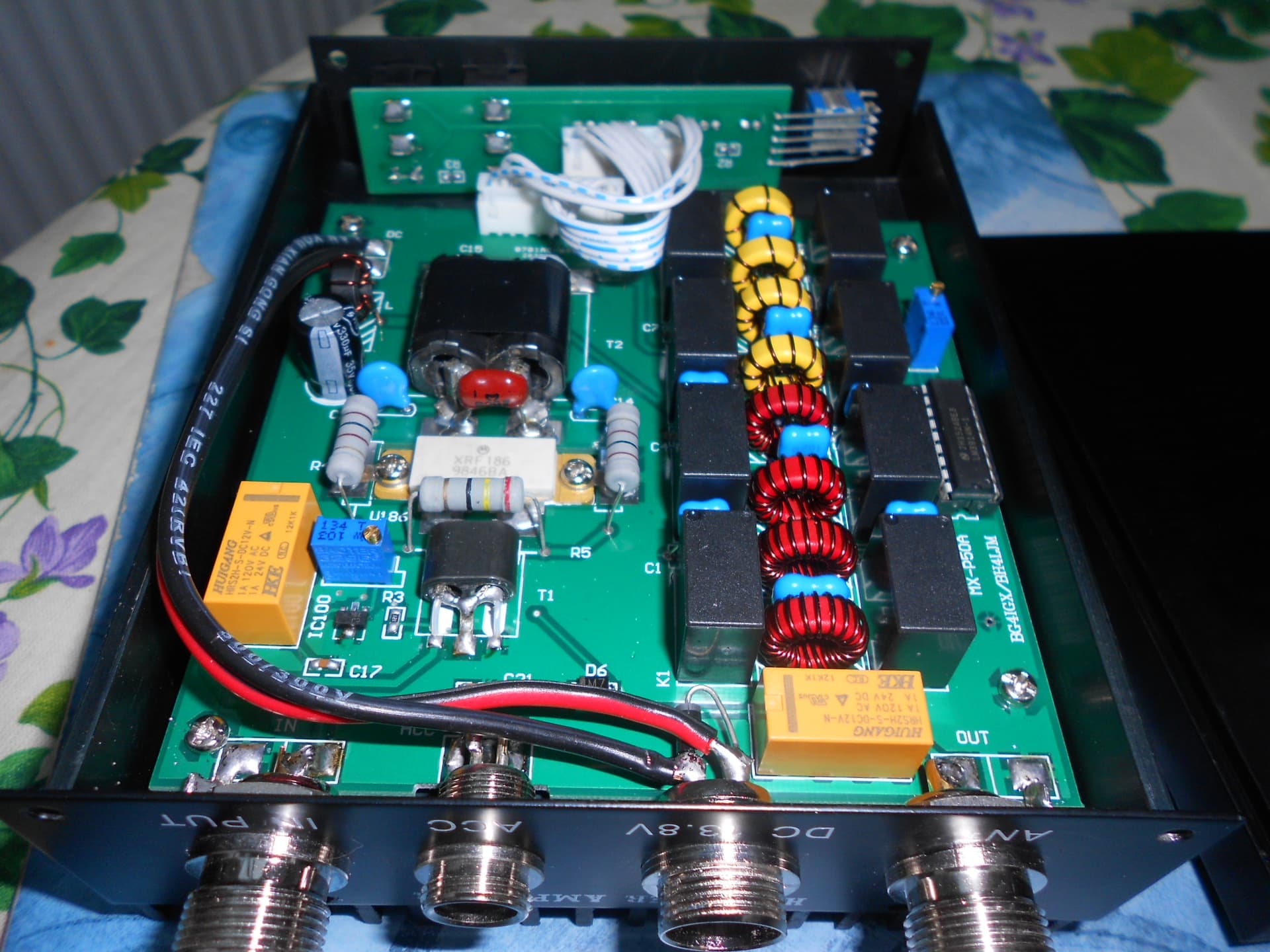
FITTING the New Device:
Cleaned everything
Ensured ALL solder was removed from the PCB pads so that the terminal tags on the new device sat down in intimate contact with its heatsink.
Checked for cleanliness again. (You don’t want grit in there). Applied a thin film of heatshink compound to the heatsink and a thin film to the base of the new device.
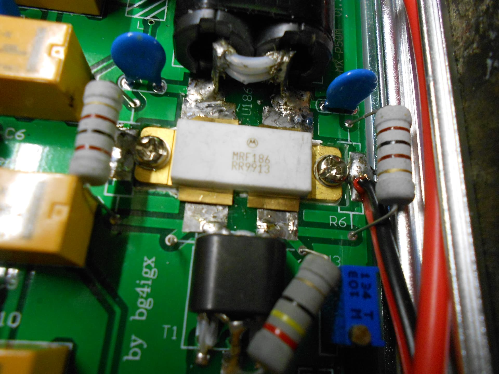
Using tweezers, placed the new device onto heatsink. Tightened the screws evenly. Excess compound squeezes out. Cleaned off.
Soldered each of the four terminal tags to the PCB pads in turn allowing for cooling between stages
Soldered the capacitor (removed earlier) across terminal tags A and B
……
TESTS on new and old devices:
Measurements using a DMM set to ‘diode drop’.
(no other connection to the device, no power or other stimulus applied):
NEW Device:
NEW Device with labelling orientated so it can be read:
Black DMM probe on base plate.
Red DMM probe on each terminal tag in turn:
All (A,B,C,D) open circuit (no conduction to base plate)
Red DMM probe on base plate.
Black DMM probe on each terminal tag in turn:
Top two pads (A and B): 0.57 V forward drop
Lower two pads (C & D): Open circuit (no conduction)
……
BLOWN Device (guidance only):
Black DMM probe on base plate.
Red DMM probe on each terminal tag in turn:
A: Short Cct
B: Open Cct
C: 0.014
D: 0.063
Red DMM probe on base plate.
Black DMM probe on each terminal tag in turn:
A: Short Cct
B: 0.49
C: 0.014
D: 0.063
Guidance only - this was what I found on my particular blown device with my particular Beckman DMM. Obviously other devices could exhibit all kinds of different readings depending on the circumstances of failure etc. However it is worth knowing what new and blown devices check out like.
Note: I always test on FM with a power meter and dummy load connected and taking quick readings.
……
Hope this helps.
Good luck
John G4YSS
Photos: 8-10-11-14-17
Above: Removing the capacitor
Above: Cut through the terminals with a sharp knife and remove the screws.
Above: Lift out the blown item
Above: Clean off and apply heatsink compound
Above: New device screwed down and ready for soldering in.
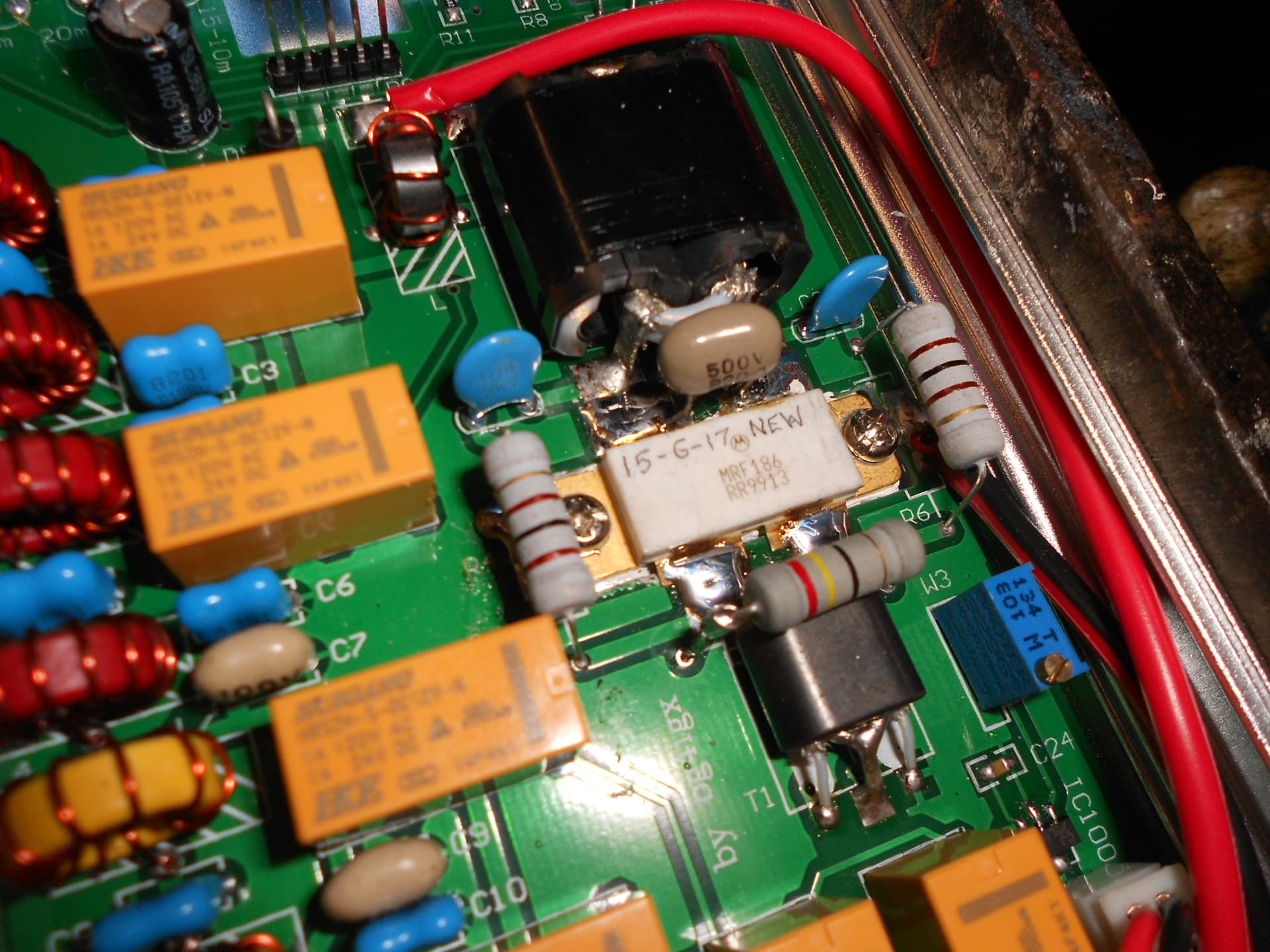
Above: Replaced