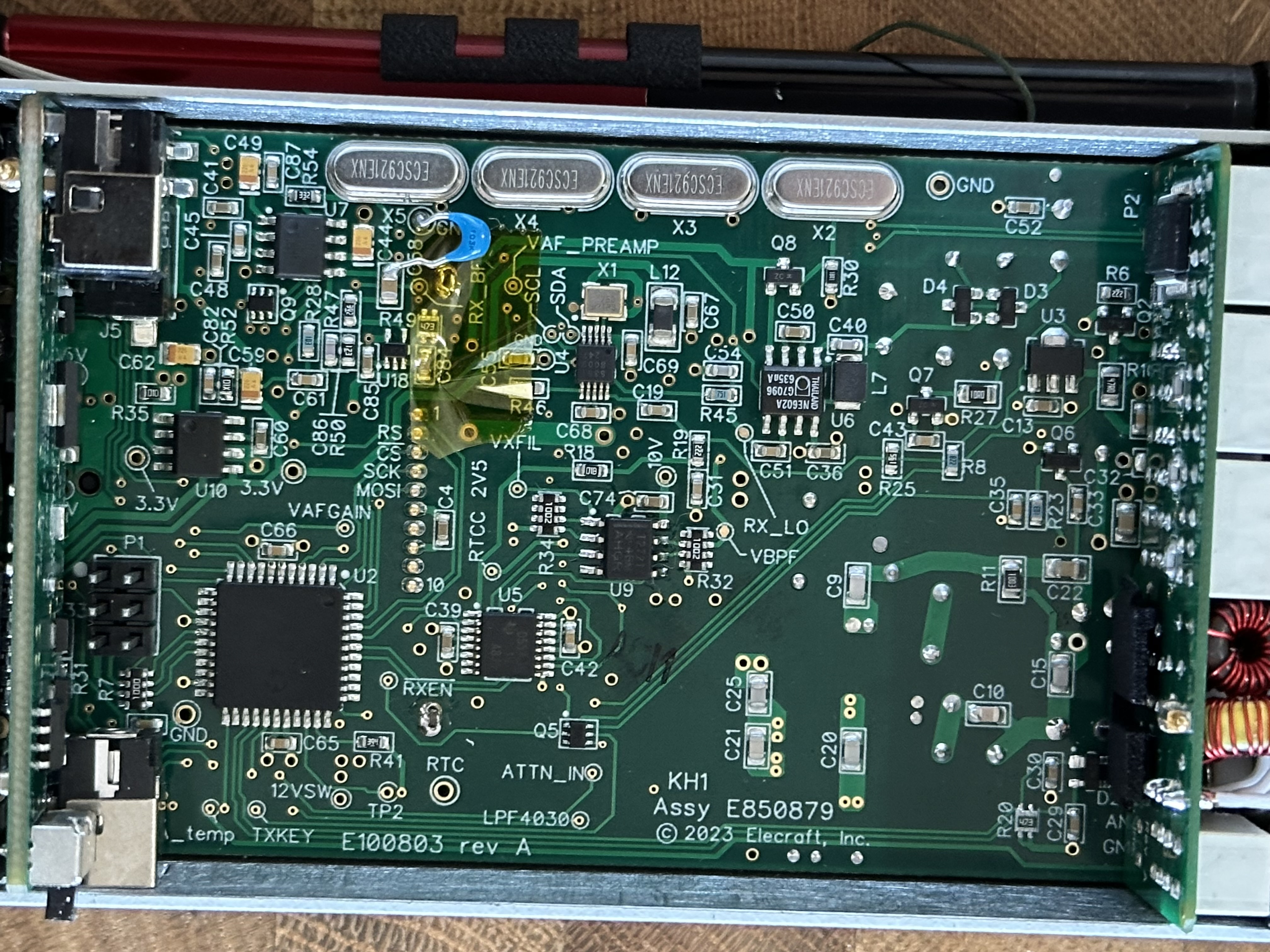
I had a chance to look inside a KH-1 while its battery was being charged.
I have to imagine that some/much of its design is drawn from Wayne’s experience with the K1/K2/KX1.
Some of the chips appear to have their labels scrubbed such as U2 (44 pin) which makes id-ing a little more difficult. As a wild guess, i wonder if U2 isn’t an ARM processor (M0?) that has replaced the more venerable PIC or whatever that has been used in the K1/K2 etc.
You can clearly see the 4 crystals and Wayne has shared its a superheat design (like teh K1/K2 etc.
What is really quite fascinating and I’d love to know the story on it is the presence of a NE602 (U6) (yes that chip….). I couldn’t find another NE602 (in the K1/K2 etc the NE602 are used to mix and match from RF to IF to baseband frequencies) but two unmarked chips have similar form factors and pin count (U7 and U10). Maybe U6 is taking the RF and mixing it down to an IF that is pushed through the 4 crystals and then U7 mixes the IF down to audio.
Maybe U4 is an SI535x family member as I can see 53 (i think) as a marking.
I’ve listened to K1/KX1 and Steve Webers variations that seem to have the 602/612 “roar” but it seemed the few minutes i listened into Fred’s QSO’s that the KH-1 was and is a “quiet” radio.
Wow! Thanks for sharing the picture Paul. I did not expect to see a 602 in the KH1. I’m guessing Elecraft must be sat on a large stock of mixer chips in order to be confident to use them in a new design.
73, Colin
Edit- yes, I’d say you were right about the SI5351, you can see labels for the I2C bus and the reference oscillator.
Agree that Elecraft might be sitting on a pile of 602.
Far from it for me to say this but maybe Elecraft (and I think Wayne said something to this effect) believe a very small number of KH-1s will be sold over its life.
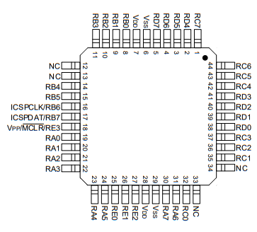
Pretty sure that’s still a PIC. 18F series (among others) comes in TQFP44 and that big .1" 6-pin header is a dead giveaway as an ICSP port. ARM use SWD headers that are usually 8 pin .05" these days. Pinout seems to match:
In the lower left of the PCB, P1 is a 6 pin header in .1", which is still standard for ICSP. Microchip also recommends 100ohm serial resistors as ESD protection, which is the R7 resistor pack.
The standard ICSP header pinout is:
1 = VPP/MCLR
2 = VDD Target
3 = VSS (ground)
4 = ICSPDAT
5 = ICSPCLK
6 = No Connect
The pins from the MCU to the rpack appear to be 16-ICSPCLK, 17-ICSPDAT, and 18-VPP/MCLR, which trace up into the header, even if it’s not clear exactly which net goes to which header pin.
The pattern of No Connect pins on the PCB also seems to match the package NC locations, along with the decoupling caps C65 and C66 at Vss-VDD. I haven’t taken the time to map out peripheral locations (SPI and I2C), but that would probably help narrow down the specific model. This could be one of a couple dozen or so models in the PIC18F family. I believe it’s not a PIC16F since those only have a single peripheral that can be configured as either I2C or SPI, whereas the 18F has two separate peripherals for those buses.
Also some further I/O guessing: the 10 through-hole points at center-left marked 1/RS/CS/SCK/MOSI/…/10 likely control the display using SPI, provide power to the display, and return the front panel button inputs.
The THEORY OF OPERATION says ‘Local oscillator signals for both the LO and BFO are synthesized by a specialized IC that generates signals in the GHz range, then divides them down to HF’ – I suspect this is a reference to the internal architecture of the si5351, as it looks like one of the clocks goes direct to the clearly labeled NE602, which has a labeled test point ‘RX_LO’ coupled via a series C to pin 6, NE602 LO input. So I reckon this is the first mixer. This is further evidenced by pin 4 (output) going to Q8 base, emitter (emitter follower) to the right hand end of the crystal filter chain.
To the left of the si5351 is a label RX_BFO partially obscured by a 100n post pick-n-place capacitor. Guessing U7 is another NE602 as product detector, and U10 is a dual opamp for audio filtering and amplification.
D3 and D4 are dual diodes, maybe for mixer protection?
There should also be a digital volume control (digipots) somewhere in this area.
Also from the manual – ‘a 32 K EEPROM for decoded TX text logging; and a real-time clock IC (RTC).’
U5 is EEPROM ? U9 Realtime clock?
The absence of a topside ground plane infill is surprising.